8-Bit Sequential Processor

A working CPU built from wires, gates and logic components inside Logic World.

A custom 8-bit computational system designed from first principles to make arithmetic, memory, control logic and clocking tangible. Version 1 is complete and executes Fibonacci using hardwired sequential control; version 2 is in development.

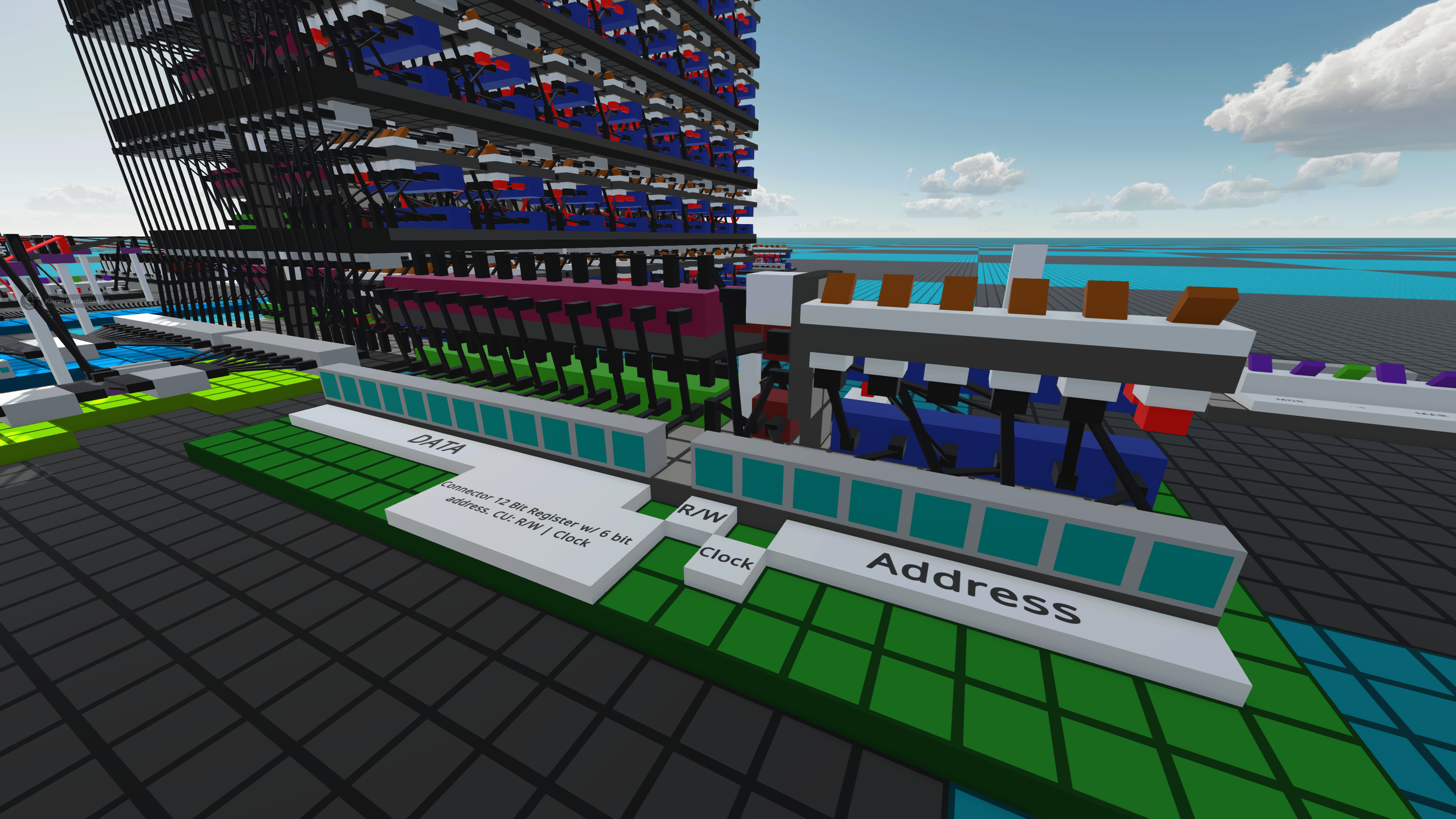
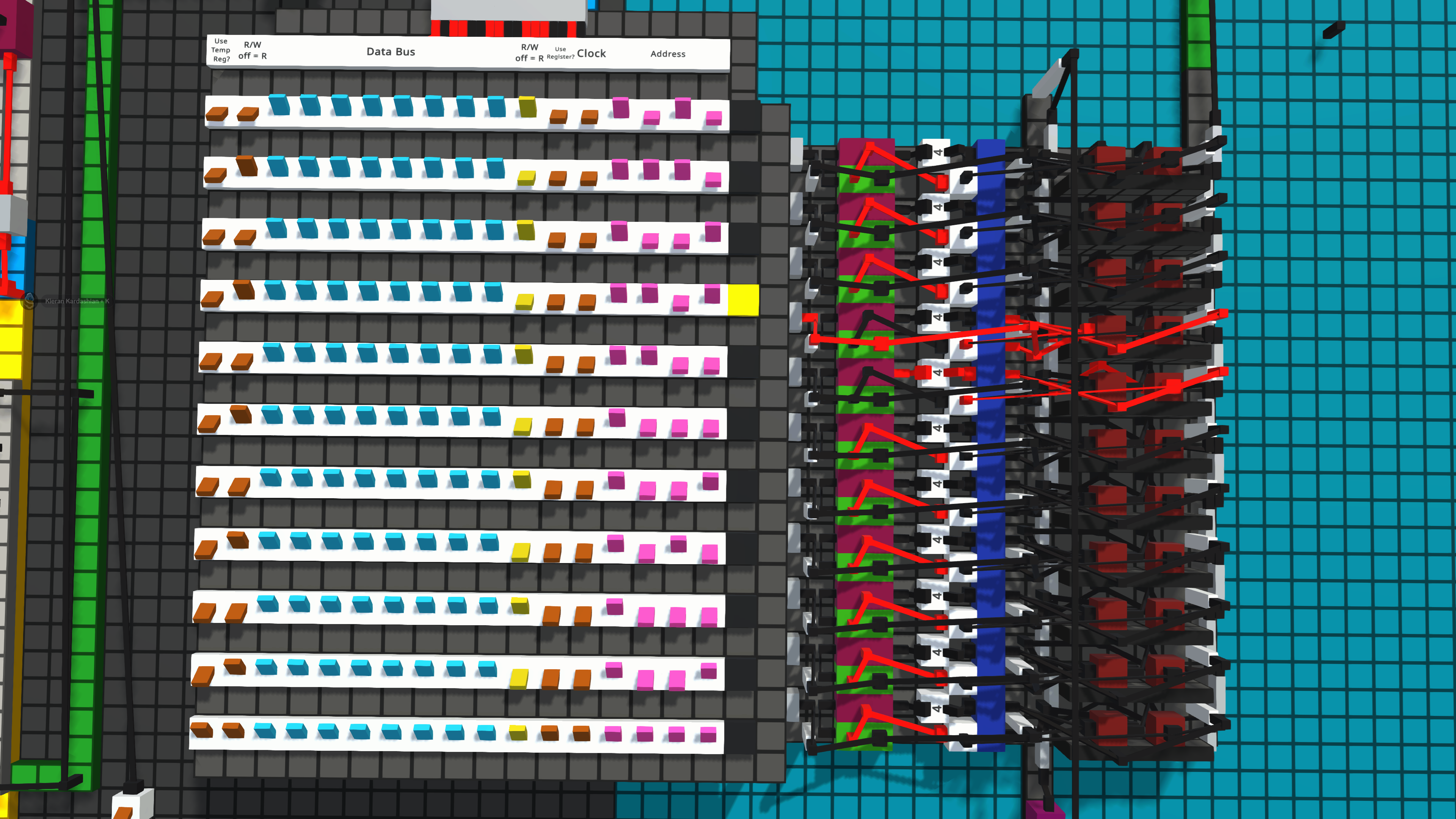
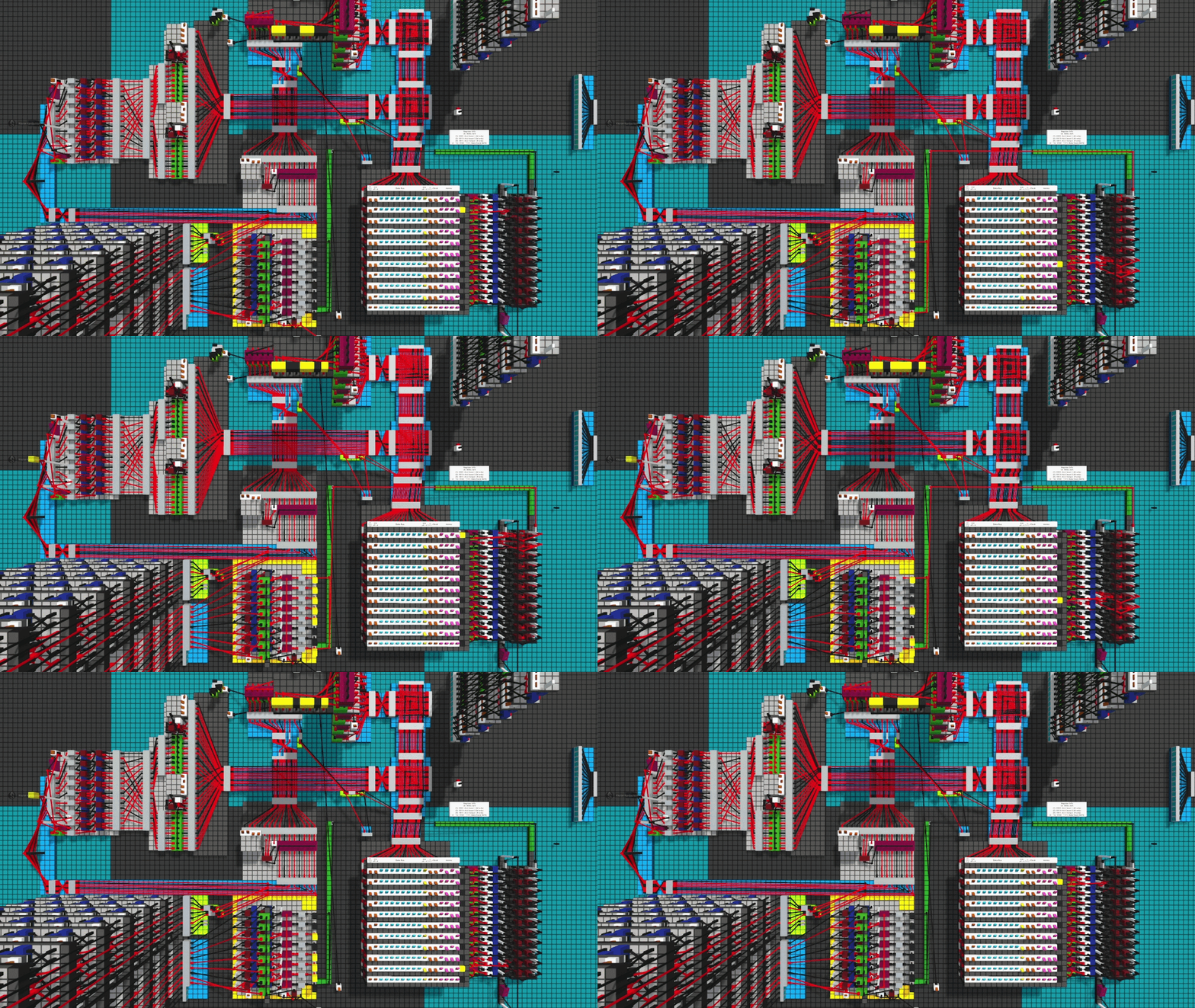
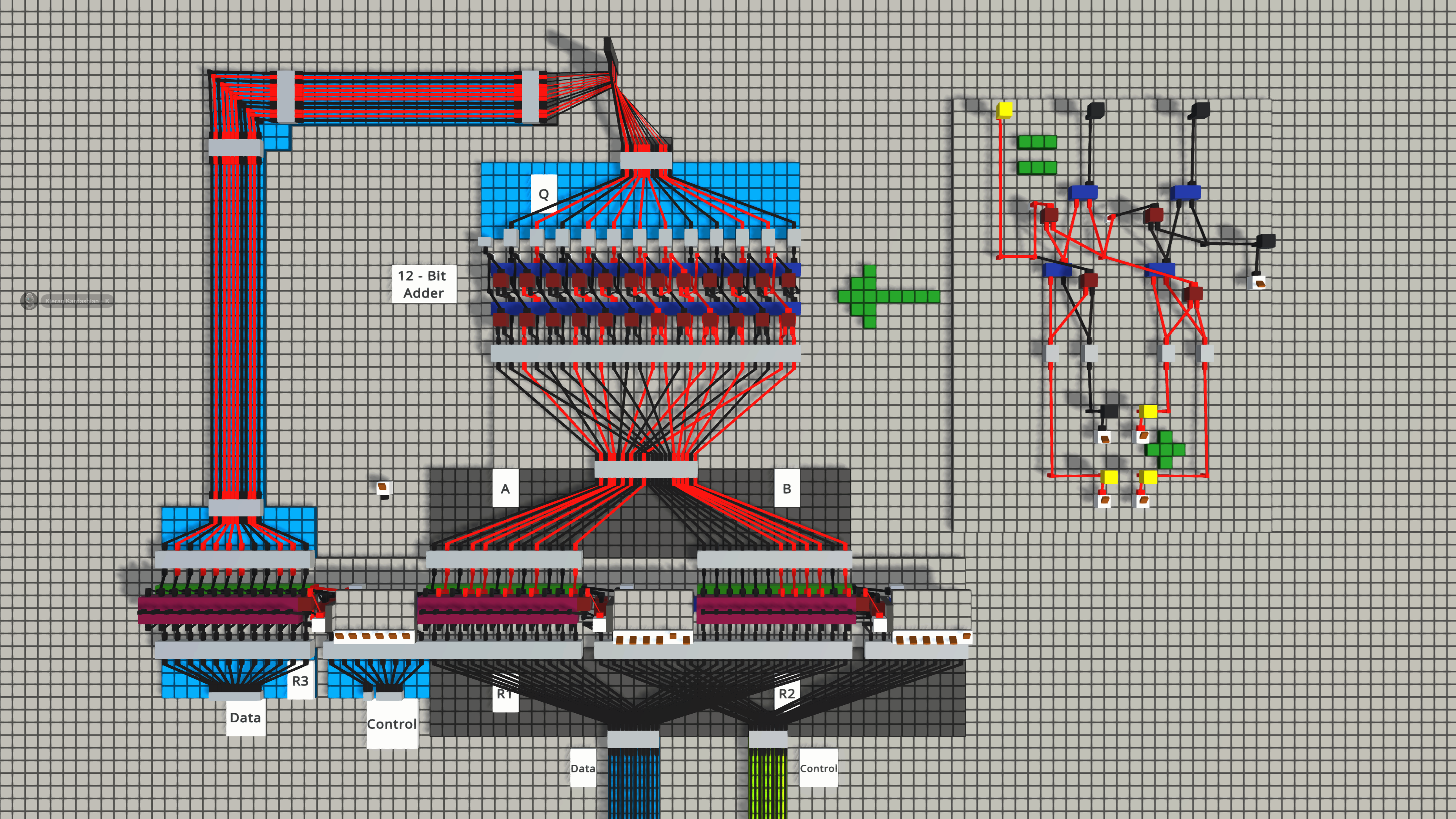
Full view of the 8-bit sequential processor inside Logic World
CPU // Full Build Overview LOGIC_WORLD · 8-BIT · SEQUENTIAL

What the system does

From individual gates to a working computation

Version 1 executes a Fibonacci sequence using a modular hardwired instruction chain. The ALU, memory, registers, buses, clock and control logic were all designed and wired manually inside Logic World rather than assembled from prebuilt processor modules.

The goal was not simply to reproduce a textbook diagram. It was to build something that had to behave correctly at the signal level, where timing mistakes, bus conflicts and a single incorrect bit could break the whole computation.

Version 2 is under development and is intended to add more capable execution control, branching, indirect addressing and a wider instruction set.

Why I built it

I wanted to understand how computers work underneath the abstraction layers - not only how to write code for a processor, but how the processor itself stores state, moves data, performs arithmetic and coordinates operations.

Building from individual logic components removes the compiler, framework and operating system that normally hide those details. Every signal transition and timing decision becomes an engineering problem you can see.

The project began with binary addition and grew into a complete sequential system with memory, registers, control logic and a functioning execution cycle.

“At some point, I realised I had accidentally started building an actual computer.”

System specification · v1

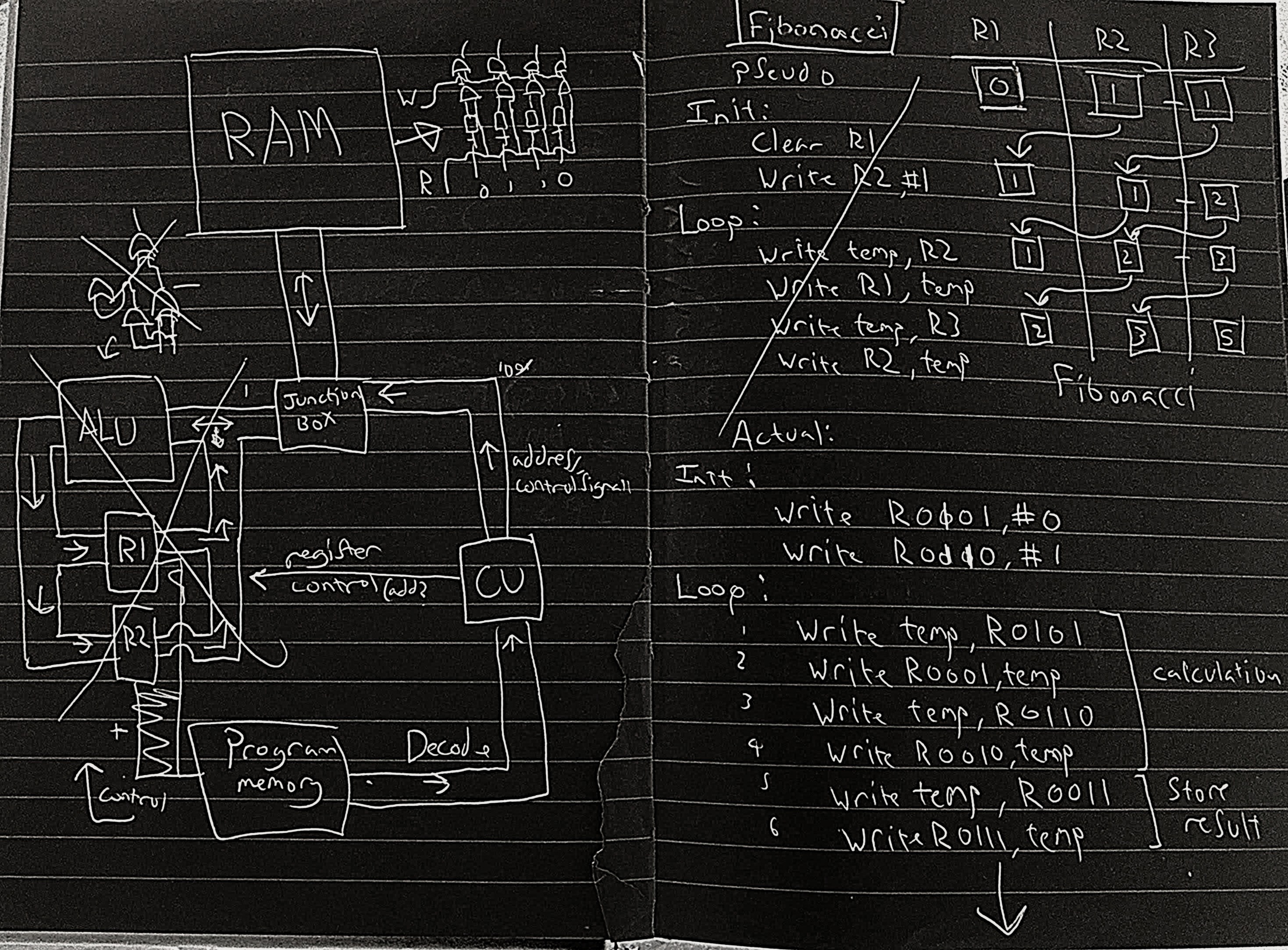
Hand-drawn planning diagram for the v1 CPU architecture
FIG 1 — pre-v1 architecture planning · Von Neumann · Fibonacci execution

Architecture

PROCESSOR_TYPE: Sequential hardwired computation

DATA_WIDTH: 8-bit

ADDRESS_WIDTH: 4-bit (16 address positions)

BUS_ARCHITECTURE: Von Neumann shared data/instruction bus

CLOCK_SYSTEM: Automatic with manual step override

ENVIRONMENT: Logic World
Memory

ADDRESS_SPACE: 16 positions

IMPLEMENTED_MEMORY: 8 bytes in v1

MEMORY_TYPE: Read/write RAM

ACCESS_METHOD: Direct addressing

REGISTERS: Accumulator, MDR and purpose-built storage registers

Control

ALU: Operational · ADD

CU: Hardwired sequential control

CLK: Automatic + manual override

BUS: Operational

OUTPUT: LED/lightboard bit visualisation

FLAGS: Overflow implemented

BRANCHING / INDIRECT ADDRESSING: Not present in v1

What it demonstrated

Engineering outcome

The project turned registers, buses, clock cycles and instruction execution from abstract concepts into practical engineering problems. Building even simple functionality at hardware level made the cost of every abstraction much more obvious.

  • Designed and implemented a working sequential processor architecture.
  • Built modular memory, ALU and control subsystems from logic components.
  • Executed a real iterative computation: Fibonacci generation.
  • Developed systematic debugging strategies for signal-level faults.

Next steps

Version 2 is the next major milestone. The current direction is to expand the instruction set, add branching and indirect addressing, and replace the fixed v1 execution chain with more capable control logic.

Longer term, the project is a platform for exploring larger address spaces, richer ALU operations and more conventional processor architectures.

More detail

Project status

v1: complete and stable, with the Fibonacci demonstration working end-to-end.

v2: active development. The page will evolve as the architecture becomes more capable.

The claims on this page intentionally distinguish completed v1 functionality from planned v2 features.